Elegance of Thin Film Resistors
Thin film resistors are crafted through vacuum deposition, layering a uniform metallic film on an insulating substrate for precise electrical conduction. Known for their stability, they exhibit a low-temperature coefficient of resistance, making them ideal for high-precision applications.
A Tale of Modeling and Simulation: The Thin Film Resistor
In this example, EMS plays a crucial role in accurately modeling and simulating the detailed workings of a thin film resistor. Figures 2 and 3 serve as visual aids, revealing the complex geometrical parameters and the 3D simulation of the resistor, showcasing its intricate design.
.
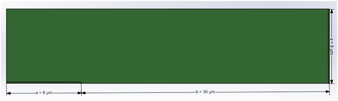
Figure 2 - Model dimensions
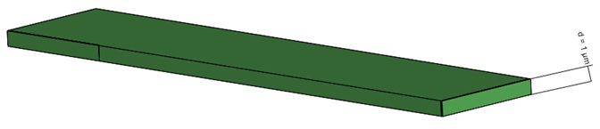
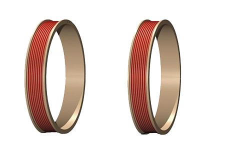
Figure 3 - 3D Model of thin film resistor
Electric Conduction Simulation
The Electric Conduction module, a key component of EMS, is adept at calculating current flow in conductors caused by voltage differences. It provides a suite of outputs such as electrostatic potential, field, current density, breakdown voltage, and resistance, enabling comprehensive analysis. This module also integrates with thermal and motion studies, broadening its application scope.
In a highlighted example, the Electric Conduction Module calculates resistance, defined as the voltage-to-current ratio, within EMS. It involves setting entry and exit ports for the current's pathway through the resistor. EMS calculates the voltage difference between these ports and tracks the current's path, accurately determining resistance. This process highlights EMS's capability to elegantly derive resistance values, showcasing its analytical prowess.
Simulation Setup
To conduct an Electric Conduction simulation in EMS, follow these concise steps:
1. Create a New Electric Conduction Study: Initiate by setting up a new study specific to electric conduction within EMS to analyze current flow and resistance in conductors due to voltage differences.
2. Apply Suitable Materials to the Parts: Assign appropriate materials to each part of your model, considering their electrical properties such as conductivity and permittivity, which are critical for accurate simulation results.
3. Apply Suitable Load and Restraint: Define the electrical loads (e.g., voltage or current inputs) at specific points or surfaces and apply necessary restraints to simulate real-world conditions and interactions accurately.
4. Mesh and Run the Simulation: Generate a mesh that accurately represents the geometry of your model, then run the simulation to compute the desired electrical properties and analyze the behavior of your design under the applied conditions.
Materials
In this case, the thin film resistor is made of metallic material with 2e+7 S/m conductivity.
Load Restraints
Figure 4 illustrates the application of fixed voltages on specific faces: 0.001V on the left face and -0.001V on the right face, with resistance parameters also set on these faces.
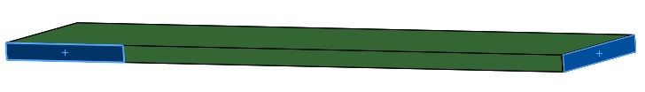
Figure 4 - highlights of faces where fixed voltages and resistances are applied
Mesh
Meshing, crucial in finite element method (FEM) simulations, affects accuracy and computation time. Finer meshes yield more precise results but increase computational demands. EMS offers automatic mesh generation based on the model's size and allows for customized mesh sizes on solid bodies and faces. In our example, critical faces with fixed voltages are finely meshed with a maximum element size of 0.1 µm, while the overall model adheres to a maximum size of 0.3 µm, as showcased in Figure 5.
FEM Results
After executing the study, EMS generates results with an option to enhance accuracy by switching from "Normal" to "High" accuracy in the advanced study properties. While high accuracy increases solving time, it significantly improves result precision.
The resistance of the thin film resistor is determined using the following formula [1]:
$$ R = \left( \frac{b}{a} + 0.469 \right) \cdot (\sigma \cdot d) $$
$$ R = \left( \frac{30}{8} + 0.469 \right) \cdot \left( 2 \times 10^7 \times 1 \times 10^{-6} \right) $$
$$ R = 2.1095 \times 10^{-1} \, \Omega $$
Figure 6 reveals the resistance value calculated by EMS using the finite element method, showcasing a remarkable alignment with theoretical predictions. Figures 7 and 8 display 3D plots of current density and electrostatic potential, respectively, illustrating the detailed outcomes of the simulation.
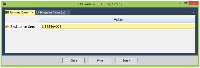
Figure 6 - Resistance calculated by EMS
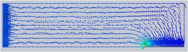
Figure 7 - Current density, vector plot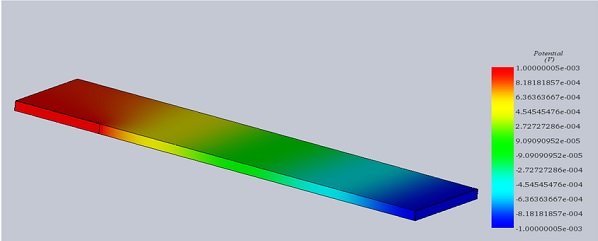
Figure 8 - Potential plot
Harmony Between Analytical and EMS Results
The analytical results for thin film resistance align closely with the findings from EMS. As part of EMWorks' suite specializing in low-frequency analysis, EMS integrates with leading 3D CAD software, including Autodesk Inventor, providing engineers with advanced tools to optimize their designs effectively, leading to notable savings in both time and costs.
Conclusion
This application note delves into the precision modeling and simulation of thin film resistors using the EMS Electric Conduction module, highlighting its integration with advanced 3D CAD software for optimal design efficiency. Thin film resistors, known for their stability and low-temperature coefficient of resistance, are meticulously crafted through vacuum deposition, making them suitable for high-precision applications.
EMS plays a pivotal role in simulating these resistors, focusing on calculating resistance—a critical parameter defined by the voltage-to-current ratio. The simulation process is detailed, from creating a new Electric Conduction study and applying suitable materials with specific electrical properties to defining electrical loads and accurately meshing the model for precise results. The material for the resistor, a metallic substance with a conductivity of \(2 \times 10^7\) S/m, is carefully selected to reflect real-world conditions.
Figures accompanying the note, including the application of fixed voltages and the meshing approach, illustrate the rigorous attention to detail in simulating the resistor's behavior under electrical stress. The note concludes that EMS’s simulations closely match theoretical expectations, offering significant time and cost savings in engineering designs. This synergy between analytical findings and EMS results underscores the module's capability to enhance the design and optimization of electronic components, particularly thin film resistors, for high-precision applications.
References
[1]: Conformal Mapping: Methods and Applications, Roland Schinzinger, Patricio A. A. Laura, 1991, Elsevier Science Publishers, B.V., p. 224. ISBN 0-486-43236-X (pbk).