Parasitic parameters of a PCB
Parasitic capacitance, parasitic resistance, and parasitic inductance
In Electronic Design Automation (EDA), parasitic extraction involves calculating parasitic effects such as capacitance, resistance, and inductance in electronic circuits and interconnects. This article demonstrates the use of EMS to compute these circuit parameters and compares the results to published data [1].
PCB CAD model
- Copper Conductivity = 5.8 x 10^7 S/m
- Relative Permittivity of FR4 = 4.4
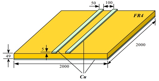
Figure 1 - A PCB structure used for simulation where all dimensions are in mils
Capacitance calculation
To calculate the parasitic capacitance of the PCB structure depicted in Figure 1, the Electrostatic module is utilized. Figure 2 displays the model and mesh for the PCB structure.
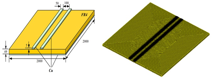
Figure 2 - Model and mesh of the PCB structure
Three floating conductors
To calculate the capacitance of a specific conductor, it is assigned a floating boundary condition, including the ground plane, in EMS. Consequently, this PCB structure has three floating conductors: the left and right traces, as well as the ground plane.
Figure 3 and Table 1 display the capacitance results from EMS alongside those from Reference [1].
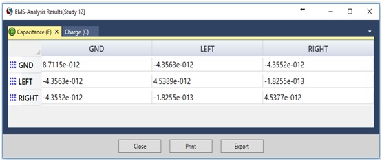
Figure 3 - Parasitic capacitance computed by EMS
| Reference [1] | EMS | |
| The capacitance between the left trace and the ground plane | -4.3047 pF | -4.3563 pF |
| The capacitance between the right trace and the ground plane | -4.3046 pF | -4.3552 pF |
| The capacitance between the two copper traces | -0.1673 pF | -0.1825 pF |
DC Inductance & DC Resistance calculation
To calculate the DC resistance and inductance of the PCB structure in Figure 1, the EMS Magnetostatic module is utilized. In this case, the copper traces are modeled as coils to compute their DC inductance and resistance. The results obtained by EMS for DC inductance and resistance are compared to those from Reference [1], as presented below:
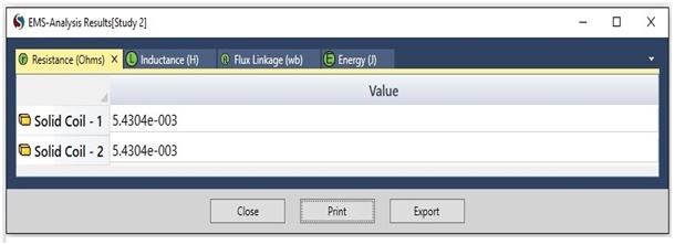
Figure 4 - DC Resistance computed by EMS
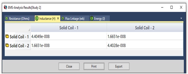
Figure 5 - DC Inductance computed by EMS
DC loop Inductance is obtained by the following formula:
L Loop = L11+L22- 2*M12 ; where L11, L22: self inductances; M12: mutual inductance
| Reference [1] | EMS | |
| DC resistance | 5.4304 m Ohm |
5.4304 m Ohm |
| DC Loop inductance | 50.742 n Henry |
54.775 n Henry |
AC Inductance & AC Resistance calculation
In addition to DC inductance and resistance calculations, EMS offers AC Magnetic and eddy current capabilities. These features are utilized to compute the AC resistance and AC loop inductance of the PCB structure at various frequencies, including 1 kHz, 2 kHz, 5 kHz, 10 kHz, 20 kHz, 50 kHz, 100 kHz, 200 kHz, 500 kHz, and 1 MHz.
Reduced model
Due to the small size of the skin depth in the conducting regions (approximately 1e-005 to 1e-004 mm), significant computational resources, including CPU and RAM, are required. As a result, only 1/20 of the model is simulated, as depicted in Figure 6. Subsequently, the inductance and resistance values obtained from the reduced model are multiplied by 20 to derive the results for the full model.
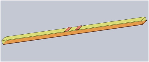
Figure 6 - 1/20 of the structure is modeled for AC Magnetic analysis
Similar to the previous Magnetostatic analysis, the two traces are modeled as coils. To consider the skin depth in the AC resistance calculation, the coils are modeled as solids, as wound coils do not support eddy currents. Figure 7 displays the AC resistance results for frequencies ranging from 1 KHz to 1 MHz, computed by EMS and compared to Reference [1]. Figure 8 presents the AC inductance results and comparisons for the same frequency range.
![AC resistance computed by EMS and compared to Reference [1]](/ckfinder/userfiles/images/AC-resistance-comparison.png)
Figure 7 - AC resistance computed by EMS and compared to Reference [1]
![AC inductance computed by EMS and compared to Reference [1]](/ckfinder/userfiles/images/AC-inductance-comparison.png)
Figure 8 - AC inductance computed by EMS and compared to Reference [1]
Conclusion
This application note explores the critical role of EMS in modeling Electromagnetic Interference (EMI) by extracting parasitic parameters from PCBs to predict high-frequency circuit behaviors. It focuses on calculating parasitic capacitance, resistance, and inductance, demonstrating EMS's effectiveness through comparisons with published data. The note details a simulation of a PCB structure with copper traces on an FR4 board, utilizing EMS for both DC and AC analyses. Capacitance calculations are performed using the Electrostatic module, while DC resistance and inductance are calculated with the Magnetostatic module. For AC parameters, due to the small skin depth, a reduced model is simulated, and results are scaled to represent the full model. The findings show close alignment with reference data, highlighting EMS's precision in simulating parasitic effects, crucial for designing circuits with minimized EMI. This work underscores the importance of accurate parasitic parameter extraction in developing efficient electronic designs for advanced applications.
References
[1] Jingen Qian, “RF Models for Active IPEMs”, MS Thesis in Electrical Engineering, Virginia Polytechnic Institute and State University, January 31, 2003.