A Bandpass Filter
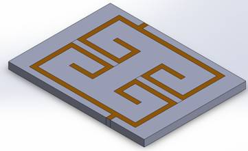
Figure 1 - Coupled microstrip filter
.PNG)
Figure 2 - All dimensions are in mm
Simulation
The Scattering Parameter simulator was employed, utilizing a precise frequency plan characterized by a small step size. The frequencies are uniformly distributed within the range of 2 to 3 GHz for accurate and comprehensive analysis.
Solids and Materials
The microstrip lines were fabricated on a substrate featuring a relative permittivity of 3.3. Beneath the substrate, there exists an ultra-thin layer, effectively treated as a Perfect Electric Conductor (PEC) surface. As microstrips inherently do not facilitate TEM propagation, especially with the air layer above the conductor, an air box is incorporated to establish heterogeneity between these two media, ensuring accurate modeling of the electromagnetic interactions.
Load/ Restraint
Ports are strategically placed in proximity to the microstrip line's starting and ending points, enabling precise measurement and analysis. The ground metal is designated as a Perfect Electric Conductor (PEC), ensuring realistic simulation of electromagnetic interactions and wave propagation within the structure.
Meshing
To ensure accurate simulation results, the mesh is meticulously refined around the port and RF carrier conductor. Additionally, the gap between conductor segments is finely meshed, enhancing the simulation's ability to capture electromagnetic behavior with high precision.
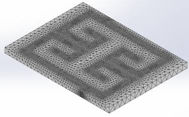
Figure 3 - Mesh of the Microstrip Filter
Results
A wide array of 3D and 2D plots is at the user's disposal, catering to the specific requirements of the task and the parameters of interest. In the context of filter simulation, it is beneficial to plot the reflection coefficient alongside the insertion loss, which aids in assessing impedance matching efficiency and filter performance.
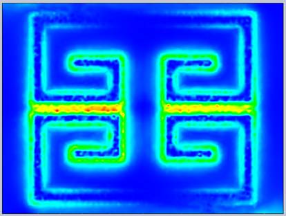
Figure 4 - Near Electric Field distribution at 2.54 GHz
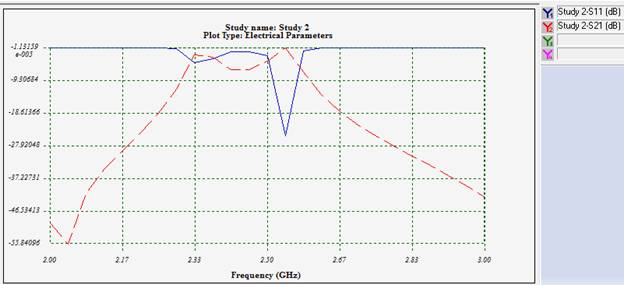
Figure 5 - Variations of reflection coefficient at the filter's input port
The filter achieves its best matching performance at 2.54 GHz, characterized by an exceptionally low return loss. For smoother plots, optimizing the frequency step and narrowing the frequency interval is recommended. Additionally, the option to visualize the input reflection coefficient on a Smith Chart provides a comprehensive view of impedance matching and aids in fine-tuning the design.
Conclusion
The bandpass filter discussed in this application note leverages the principles of coupled lines theory, employing four microstrip resonators to achieve precise filtering around 2.54 GHz. Through meticulous design and simulation using the Scattering Parameter simulator, the filter's performance was comprehensively analyzed. Key considerations included substrate properties, port placement for accurate measurements, and detailed meshing for precise electromagnetic behavior capture. The results showcased exceptional impedance matching and low return loss at the desired frequency, indicating the filter's effectiveness. By visualizing parameters like reflection coefficient and electric field distribution, designers can fine-tune the filter for optimal performance. This application note provides valuable insights into the design and simulation process of bandpass filters, essential for various communication and signal processing applications.
References
[1] Electromagnetic Waves and Antennas, Sophocles J. Orfanidis ECE Department Rutgers University