A Compact Planar Crossover
Crossovers, key in monolithic Integrated Circuits (ICs) and antenna arrays, enable two signal paths to cross with high isolation. Types include air bridges, bond wires, and printed planar crossovers, essential for layer-to-layer signal transport. Coupled transmission lines are typically used for power dividers, couplers, and filters, with recent designs incorporating loaded coupled lines with open or shorted stubs for band-pass filters and planar crossovers.
This article explores a compact planar crossover design using coupled lines, simulated with the full-wave 3D simulator HFWorks. An S-Parameters analysis details the electromagnetic behavior, highlighting design efficiency.
CAD Model
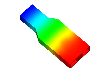
This example features a compact planar crossover design consisting of two coupled lines with two open stubs, resonating at 1.8GHz. Built on a dielectric substrate with a relative permittivity of 2.65 and a dielectric loss tangent of 0.003, the single-band crossover measures approximately 48 mm x 30 mm x 0.508 mm. A 3D model of the design is depicted in Figure 1, showcasing its compact structure and efficient use of space, optimized for high-performance applications.
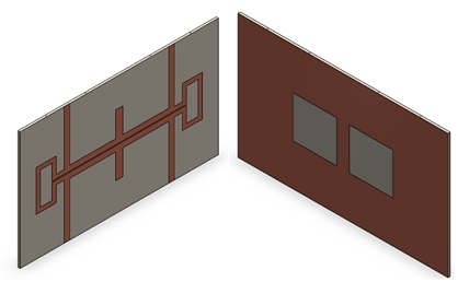
Figure 1 - CAD Model of the compact planar crossover (front and end view)
In this design, two transmission lines are interconnected at ports 1 and 4, as well as ports 2 and 3, as illustrated in Figure 2. To enhance the impedance ratio between the even and odd mode impedances of the coupled lines, the ground plane of the structure employs a patterned ground-plane technique. This method effectively increases isolation and performance efficiency. The specific parameters of the structure, detailing dimensions and characteristics, are concisely summarized in Table 1, providing a clear overview of the design specifications.
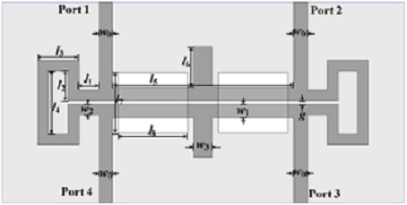
Figure 2 - The geometry of the single-band crossover
| Parameter | Value (mm) |
| l1 | 2 |
| h2 | 4 |
| l3 | 5.05 |
| l4 | 8.2 |
| w0 | 1.4 |
| w1 | 1.35 |
| w2 | 1.05 |
| w3 | 1.81 |
| g | 0.2 |
Table 1 - Structure parameters
Simulation Results
The simulated S-parameters (S11 and S31) of the single-band crossover, obtained using HFWorks, alongside the measured results, are displayed in Figure 4. These parameters are illustrated over a frequency range from 0.5 GHz to 3.5 GHz, highlighting the crossover's performance across a broad spectrum. The central frequency of the device is pinpointed around 1.8 GHz, indicating the design's optimal operational point. This comparison between simulated and measured results provides valuable insights into the accuracy of the simulation and the crossover's effectiveness at its resonance frequency.
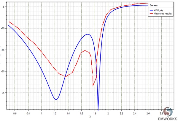
Figure 3 - The return loss S11 measured and simulated results
For the frequency range of 1.81 - 1.875 GHz, the transmission coefficient |S31| exceeds -0.6 dB, indicating efficient signal transmission through the crossover. Simultaneously, the simulated reflection coefficient |S11| is maintained below -20 dB, demonstrating minimal signal reflection and high match quality at these frequencies. This performance highlights the crossover's effectiveness in ensuring strong signal transfer with minimal loss and reflection within its operational bandwidth.
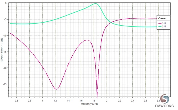
Figure 4 - S11 and S31 of the single band crossover
The isolation levels, represented by |S21| and |S41|, are maintained below -20 dB within two distinct frequency ranges: 1.73 - 1.814 GHz for |S21|, and 1.81 – 1.87 GHz for |S41|, as depicted in Figure 5. This demonstrates the crossover's capability to effectively minimize signal leakage between non-direct paths, ensuring high isolation and reducing interference across these specific frequency bands.
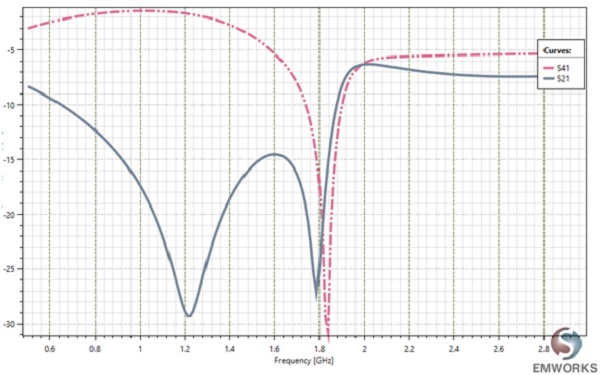
Figure 5 - S41 and S21 of the single band crossover
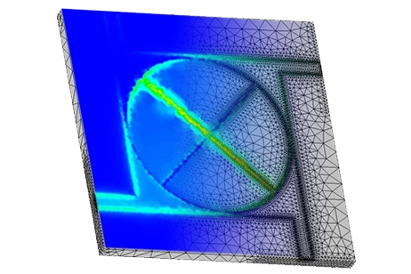
HFWorks seamlessly calculates the electromagnetic field, and the distribution of the electric field at the resonance frequency is illustrated in Figure 6, with an incident power set to 1W. This visualization provides a clear view of how the electric field propagates and distributes within the crossover at its optimal operational frequency, offering insights into the electromagnetic behavior and efficiency of the design at resonance.
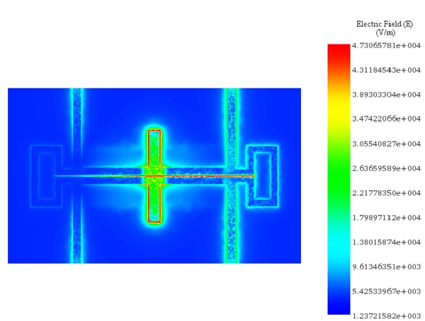
Figure 6 - Distribution of the electric field at 1.80 GHz
Conclusion
This application note introduces a compact planar crossover design optimized for high-frequency applications, specifically resonating at 1.8GHz. Utilizing a novel approach with coupled lines and open stubs, this design is simulated using HFWorks, a full-wave 3D simulator, to analyze its electromagnetic behavior through S-Parameters. The crossover, constructed on a dielectric substrate, showcases an efficient space utilization and design that enhances signal isolation and minimizes interference, crucial for monolithic Integrated Circuits (ICs) and antenna arrays.
The geometry integrates two transmission lines interconnected at strategic points to facilitate layer-to-layer signal transport with high isolation. The employment of a patterned ground-plane technique significantly improves the impedance ratio, augmenting the device's performance. Simulation results reveal the crossover's optimal performance around its central frequency of 1.8 GHz, with exceptional signal transmission efficiency and minimal reflection. Further, the device demonstrates robust isolation capabilities, effectively minimizing signal leakage and interference across specified frequency ranges.
The comparison of simulated and measured S-parameters confirms the design's effectiveness and the simulation's accuracy. Additionally, the electric field distribution visualization at the resonance frequency offers valuable insights into the electromagnetic efficiency of the crossover.
References
[1] https://www.emworks.com/product/ATLASS
[2]Wenjie Feng, Tianyu Zhang, WenquanChe“Compact Single-band Planar Crossover Based on Coupled Lines”Proceedings of the 46th European Microwave Conference, pp. 975 – 978, Oct 2016.