

パッケージ、チップ、PCB の電磁界解析
Simulate chip–package–board systems to predict impedance, delay, crosstalk, losses and EMI in high-speed electronics.
パッケージ、チップ、PCB、コネクタ、ヒートシンク、CPU、SIP、IC などのエレクトロニクス設計応用向けの電磁界ソフトウェア。
-
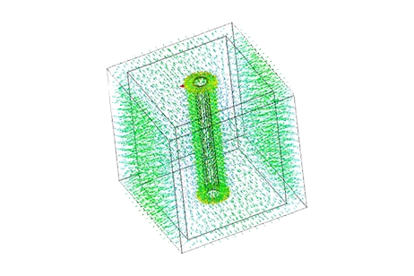
チップパッケージボードシステム
EMWorks を使用して、チップ-パッケージ-ボード システムを完全な 3D ジオメトリでシミュレーションできます。信号完全性(SI)、電源完全性(PI)、クロストーク、リターンパスを解析し、製造前に高速チャネルおよび PDN を最適化できます。 -
.webp)
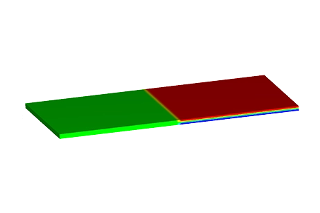
プリント回路基板(PCB)
Use EMWorks to simulate real PCB layouts, including traces, vias, planes and components. Evaluate signal and power integrity, EMI, and heating so you can fix issues and optimize stackups before fabrication. -
コンデンサ
Use EMWorks to model capacitors of any shape—parallel plate, coaxial, busbar, and custom 3D structures. Extract capacitance, visualize electric fields, evaluate parasitics, and estimate breakdown limits before building hardware.