

Microstrip to Coplanar waveguide transition
Discover how to seamlessly integrate microstrip lines with coplanar waveguides (CPWs) in hybrid circuits through our latest blog post. Using HFWorks and SolidWorks, we unveil a broadband transition design that cleverly combines microstrip-to-slotline transitions and a short-ended microstrip stub for improved impedance matching. Our discussion includes insights from HFWorks' S Parameters simulation, highlighting key performance metrics like return loss and insertion loss. Figure 1 in the post illustrates the 3D model of this innovative design, offering a practical solution for enhancing circuit integration.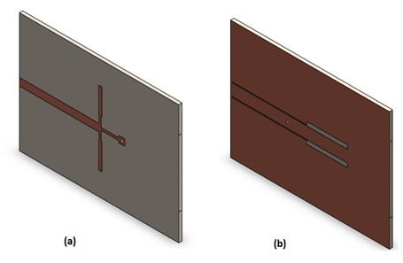
Figure 1 - 3D model of the transition from microstrip line to CPW (a) top view of the model, (b) bottom view of the model
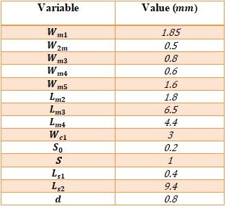
The layout of the transition from Microstrip to CPW is illustrated in Figure 2, with the geometric results summarized in Table 1.
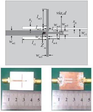
Figure 2 - Layout of the microstrip-to-CPW transition structure with a shortened microstrip stub
Simulation Results
Figure 3 presents a comparison between the simulated S parameters and the actual measurements for a single microstrip-to-CPW transition, demonstrating a strong correlation between the two. The simulation results reveal that the design achieves a return loss of better than 10 dB over a broad bandwidth ranging from 2.05 GHz to 9.96 GHz.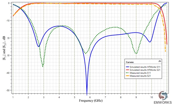
Figure 3 - Return and insertion loss of the transition from microstrip to CPW (dB)
Within the transition's passband, the maximum and minimum insertion losses recorded are 1.7 dB and 0.2 dB, respectively.