A Trimmed Resistor
Laser trimming is a precision process used in manufacturing to fine-tune electronic circuit parameters by adjusting resistor values. This involves using a laser to remove parts of a resistor, thereby increasing its resistance. This technique allows for real-time adjustments during circuit testing, ensuring optimal resistor values. The adjustment process applies to both thick and thin-film resistors on various substrates, including ceramic and surface-mounted devices, leveraging the resistor's geometry and material properties.
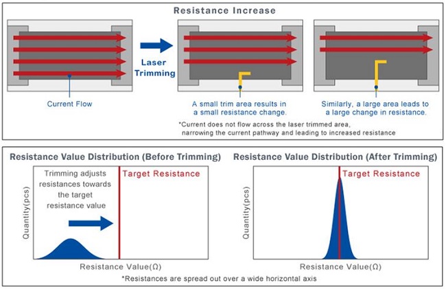
Figure 1 - Laser trimming process
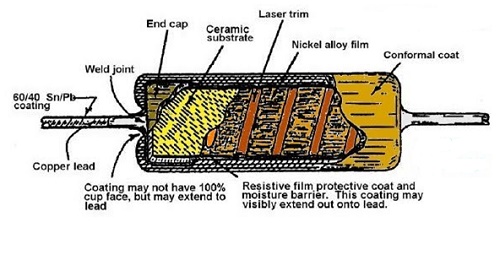
Figure 2 - Resistor cut-away
Description
To compute the resistance, electric field, current density, and potential distributions of a laser-trimmed resistor made of copper and backed by an aluminum slab with a 10-volt load applied at the extremities, an Electric Conduction analysis is required. This involves calculating the resistance based on the geometry and material properties of the copper resistor and aluminum backing. The analysis will exclude air modeling to focus on the conduction through the resistor and backing materials. This process enables the precise determination of electrical performance characteristics critical for optimizing the resistor's function in an electronic circuit.
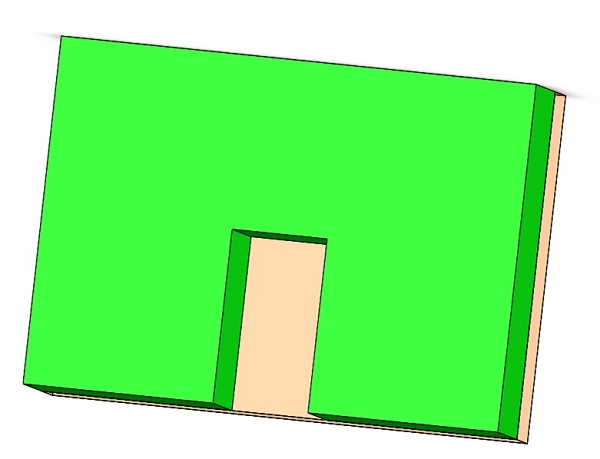
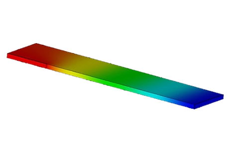
Figure 3 - 3D model of trimmed resistor
Study
To compute resistance in EMS, the Electric Conduction module is essential, calculating resistance as the voltage-to-current ratio. Users must define entry and exit points for current flow in the resistor set, allowing EMS to determine voltage difference and current. The process involves four critical steps: selecting appropriate materials, applying boundary conditions (Loads/Restraints), meshing the model, and executing the solver. This systematic approach ensures accurate resistance calculation and detailed analysis of electric conduction within the specified setup.
Materials
In EMS Electric Conduction analysis, the required properties for simulation are electrical and thermal conductivity, assuming thermal coupling is considered. This simplifies material characterization for accurate analysis, focusing on how well materials conduct electricity and, if relevant, heat.
Table 1 - Table of materials
| Components / Bodies | Material | Conductivity (S/m) |
| Trimmed | Aluminum | 38.2e+006 |
| Part 2 | Gold | 41e+006 |
Load and Restraint
In the study, specific voltage values are predefined (as detailed in a referenced table) and resistance configurations are established, which are depicted in an illustration. These parameters are crucial for conducting the analysis, and guiding the simulation's boundary conditions and objectives.
Table 2 - Applied Fixed Voltage
| Name | Fixed Voltage |
| Front Electrode | 0.6 V |
| Back Electrode | 0 V |
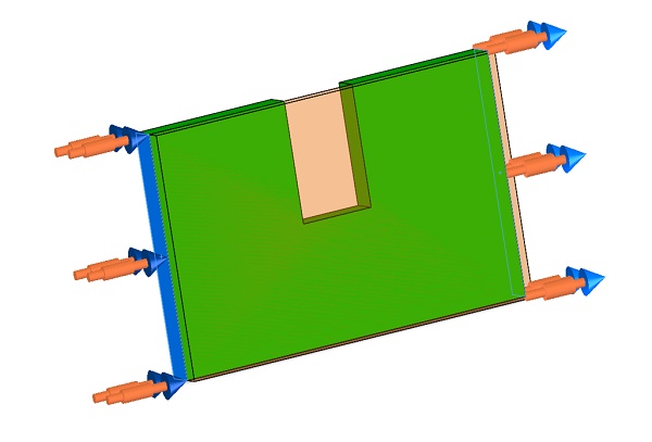
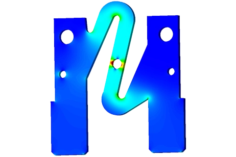
Figure 4 - Resistance Sets applied in the body where we want to calculate the resistance
Meshing
Meshing is vital in design analysis, as EMS calculates an optimal mesh size based on the model's geometry, affecting solution speed and accuracy. Larger mesh elements offer quicker, approximate results, while smaller elements are used for detailed, accurate analysis. This balance between element size and computational efficiency allows for tailored analysis precision.
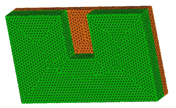
Figure 5 - Meshed Model
Results
After running the simulation, EMS provides comprehensive results, including visualizations of the Electric Field, Current Density, and Potential, alongside a detailed table summarizing resistance and dissipated power. These outputs allow for a thorough analysis of the electrical performance.
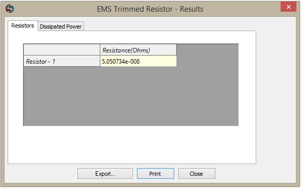
Figure 6 - Results Table
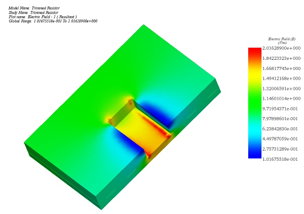
Figure 7 - Electric Field
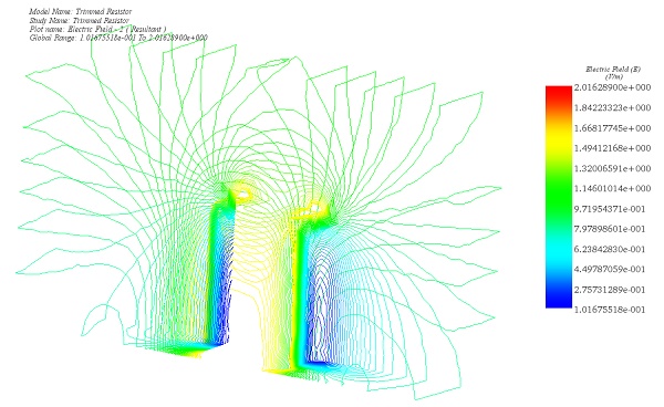
Figure 8 - Electric Field, line plot (Iso clipping)
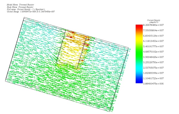
Figure 9 - Current Density, vector plot
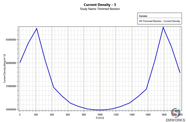
Figure 10 - Line segment plot of Current Density between two points in the opposite faces of trim
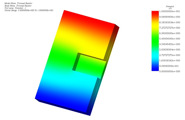
Figure 11 - Potential
Conclusion
The application note details the significance of laser trimming in adjusting resistor values for electronic circuits, emphasizing its precision and real-time adjustments during testing. The process is applicable to various resistor types and substrates, facilitating optimal circuit performance. Using Electric Conduction analysis, the resistance, electric field, current density, and potential distributions of laser-trimmed resistors are computed, focusing on copper resistors backed by aluminum. Key steps involve material selection, boundary condition application, meshing, and solver execution. EMS provides detailed results, including visualizations of electric field, current density, and potential, aiding in understanding electromagnetic properties. Overall, laser trimming offers a reliable method for fine-tuning circuit parameters, ensuring efficient electronic circuit operation.