A 3D Capacitor
The electrical characterization of 3D interconnects in VLSI has gained prominence due to the increased number of interconnect layers and higher clock speeds in contemporary VLSI systems. A key focus is on determining the capacitance matrix for 3D structures. This example demonstrates the calculation of capacitance for an interconnect comprising six conductors within seven dielectric layers, with four conductors navigating through two 90-degree bends, showcasing the complexity and necessity of accurate analysis in modern VLSI design.
.
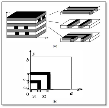
Figure 1 - Six conductors embedded in a set of seven dielectric layers
Each straight conductor has a length of 13mm. The cross-section of all conductors is 1mm × 1mm. As shown in Figure 1, the piecewise lengths of the bent conductors are a = b = 13mm, and S1 = 3.5mm, S2 = 3mm. The relative permittivity of the dielectric layers is, from the bottom, er1 = 2, er2 = 3, er3 = 3, er4 = 4, er5 = 4, er6 = 5, er7 = 5.
In the VLSI interconnect structure, each layer, except the third from the bottom, has a uniform thickness of 1mm. The third layer has a thickness of 2mm, contributing to the total structure height of 8mm. It's crucial to include air in the model to account for the surrounding environment accurately. The published article employs the domain-decomposition method (DDM) as the capacitance calculator for this interconnect configuration. Our objective is to validate EMS results against the published data [1] for capacitance calculation.
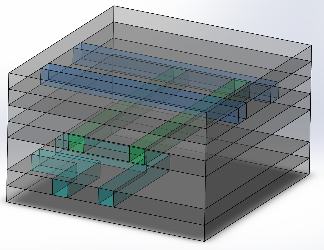
Figure 2 - Solid model of the seven layers interconnect
The study
In EMS, the Electrostatic module serves as the capacitance calculator for the 3D multilayered-interconnect structure. Following the creation of the Electrostatic study, or design scenario, three critical steps must be undertaken. Firstly, proper materials must be applied to all solid bodies involved in the analysis. Secondly, necessary boundary conditions, also known as Loads/Restraints in EMS, must be applied. Lastly, the entire model must be meshed to prepare it for simulation. These steps ensure accurate and reliable results in the capacitance calculation.
Materials
In EMS's Electrostatic analysis, the sole required material property is the relative permittivity, which dictates the electrical behavior of the materials involved. Table 1 illustrates the relative permittivity values for the seven insulating layers and the surrounding air, crucial for accurately modeling the capacitance of the interconnect structure.
|
Component/Body
|
Material Name
|
Relative Permittivity
|
|
Air
|
Air
|
1.0
|
|
Dielectric 1
|
e2
|
2.0
|
|
Dielectric 2
|
e3
|
3.0
|
|
Dielectric 3
|
e3
|
3.0
|
|
Dielectric 4
|
e4
|
4.0
|
|
Dielectric 5
|
e4
|
4.0
|
|
Dielectric 6
|
e5
|
5.0
|
|
Dielectric 7
|
e5
|
5.0
|
Table 1 - Relative permittivity of the seven insulators and the surrounding air
Loads/Restraints
Loads and restraints are essential for defining the electric and magnetic environment within the model, directly influencing the analysis results. These parameters are applied to geometric entities and are fully associative to geometry, automatically adapting to any geometric alterations.
In this study, a grounded conductor is applied to the top and bottom faces of the seventh and first dielectric layers, respectively. These conductors are indexed using floating conductors in EMS for precise control and analysis of the interconnect
Meshing
In this benchmark, meshing is relatively straightforward due to the geometry lacking small regions and gaps. Therefore, a global element size of 2 mm with a mesh tolerance of 0.1 mm is set. To ensure accuracy without significantly increasing the total number of mesh elements, mesh control is applied to regions where large variations are expected. Specifically, two local mesh controls of 0.5 mm and 0.25 mm are applied to the six conductors and dielectric layers, respectively. The resulting mesh is depicted in Figure 3.
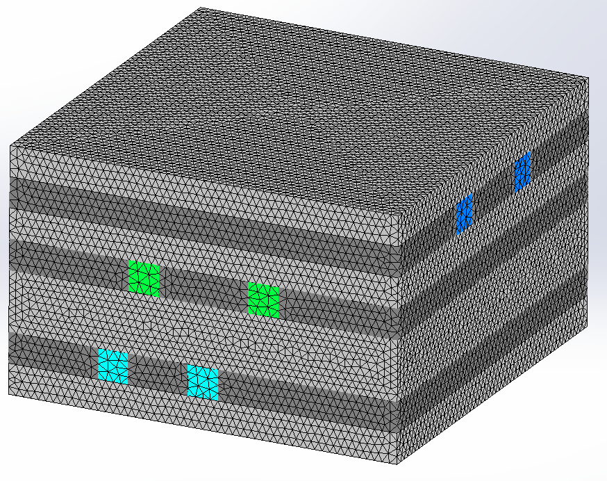
Figure 3 - Mesh of the structure without the air region
Results
After a successful run, the Electrostatic module generates three result folders and a result table. These folders contain the electric field (E), electric displacement (D), and potential distribution (V), respectively. Additionally, the results table contains the capacitance matrix. Various visualization formats such as fringe, vector, contour, section, line, and clipping plots are available for analysis, with options to zoom in, export, and dissect the results.
In this benchmark, the capacitance matrix calculated by EMS is compared against the results reported in [1]. Table 2 shows that the results obtained from EMS match those reported by the authors of [1]. EMS serves as a reliable capacitance calculator for interconnects and VLSI applications.
|
Cij (pF)
|
conductor-1
|
conductor-2
|
conductor-3
|
conductor-4
|
conductor-5
|
conductor-6
|
|
conductor-1
|
0.745
|
-0.158
|
-0.123
|
-6.515 e-03
|
-2.807 e-02
|
-4.566 e-03
|
|
conductor-2
|
-0.158
|
1.369
|
-0.210
|
-0.145
|
-3.278 e-02
|
-2.885 e-02
|
|
conductor-3
|
-0.123
|
-0.210
|
1.743
|
-0.172
|
-0.256
|
-0.262
|
|
conductor-4
|
-6.516 e-03
|
-0.145
|
-0.172
|
1.689
|
-0.265
|
-0.267
|
|
conductor-5
|
-2.807 e-02
|
-3.277 e-02
|
-0.256
|
-0.265
|
3.469
|
-5.154 e-02
|
|
conductor-6
|
-4.566 e-03
|
-2.885 e-02
|
-0.262
|
-0.267
|
-5.154 e-02
|
3.448
|
Table 2 - Capacitance matrix (in pF) obtained by EMS
|
|
C11
|
C22
|
C33
|
C44
|
C55
|
C66
|
|
DDM
|
0.680
|
1.29
|
1.57
|
1.52
|
2.54
|
2.54
|
|
Spice Link
|
0.669
|
1.29
|
1.60
|
1.54
|
2.53
|
2.53
|
Table 3 - The self-capacitance terms (in pF) as reported in [1]
Conclusion
The application note explores the critical aspect of calculating capacitance in complex 3D interconnect structures, vital for modern VLSI design. With the escalating intricacies of VLSI systems, accurate characterization of capacitance matrices is paramount. The study delves into a detailed analysis of a 3D interconnect composed of multiple conductors traversing numerous dielectric layers, illustrating the importance of precision in VLSI interconnect modeling. Utilizing EMS and the domain-decomposition method, the study successfully validates capacitance calculations against published data, affirming EMS's reliability in capacitance assessment for VLSI applications. Through meticulous steps in materials application, boundary condition definition, and meshing, EMS generates comprehensive results encompassing electric field, displacement, and potential distribution, alongside the crucial capacitance matrix. This benchmark underscores the significance of accurate capacitance evaluation in advancing VLSI design methodologies.
References
[1] Zhenhai Zhu, Hao Ji, Wei Hong, "An Efficient Algorithm for the Parameter Extraction of 3-D Interconnect Structures in the VLSI Circuits: Domain-Decomposition Method," IEEE Transactions on Microwave Theory and Techniques, vol. 45, no. 8, August 1997, pp. 1179-1184.