

Introduction
EMI, or electromagnetic interference, represents undesirable electromagnetic noise emanating from a device or system, which can interfere with the standard operations of nearby devices or systems. The core methodology for EMI modeling and forecasting entails the extraction of parasitic parameters from PCBs and their circuit components to develop high-frequency circuit models.
Parasitic Parameters
In the realm of electronic design automation (EDA), parasitic extraction involves determining the unintended parasitic effects within the devices and the necessary wiring interconnects of an electronic circuit. This encompasses parasitic capacitance, resistance, and inductance. This article showcases the application of EMS for calculating these critical circuit parameters, with a comparison of the outcomes against established data [1].
PCB structure Modeling
The PCB structure depicted in Figure 1 features two copper traces on a 4-oz FR4 square board, accompanied by a copper Ground layer with a thickness of 5 mils. The simulation incorporates specific parameters, all measured in mils, including the conductivity of copper and the relative permittivity of FR4 at 4.4.
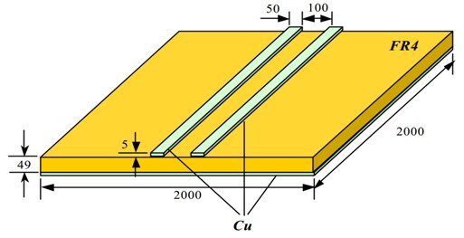
Figure 1 - A PCB structure used for simulation where all dimensions are in mils
Capacitance calculation
To calculate the parasitic capacitance of the PCB structure presented in Figure 1, the Electrostatic module is utilized. Figure 2 illustrates the model and the mesh configuration for the PCB structure.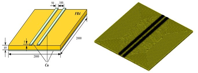
Figure 2 - Model and mesh of the PCB structure
Three floating conductors
In EMS, to consider the capacitance of a specific conductor, it is assigned a floating boundary condition, which applies to the ground plane as well. Consequently, this PCB structure comprises three floating conductors: the left trace, the right trace, and the ground plane. The capacitance results obtained from EMS and those from Reference [1] are displayed in Figure 3 and Table 1, respectively.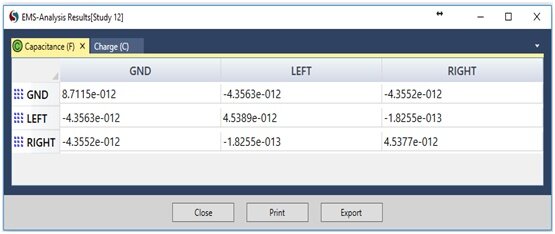 Figure 3 - Parasitic capacitance computed by EMS
| Reference [1] | EMS results | |
| the capacitance between the left trace and the ground plane | -4.3047 pF | -4.3563 pF |
| the capacitance between the right trace and the ground plane | -4.3046 pF | -4.3552 pF |
| the capacitance between the two copper traces | -0.1673 pF | -0.1825 pF |
Table 1 - Capacitance results of EMS compared to Reference [1]
DC Inductance & DC Resistance calculation
To calculate the DC resistance and inductance of the PCB structure depicted in Figure 1, the EMS Magnetostatic module is engaged. For the purpose of computing the DC inductance and DC resistance of the copper traces, they are modeled as coils within the simulation. The results for DC inductance and DC resistance, as determined by EMS and compared to Reference [1], are presented below: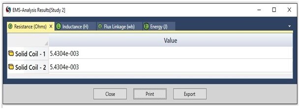
Figure 4 - DC Resistance computed by EMS
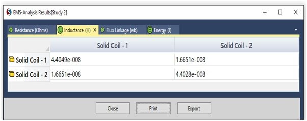
Figure 5 - DC Inductance computed by EMS
DC loop Inductance is obtained by the following formula: L Loop = L11+L22- 2*M12 ; where L11, L22: self inductances; M12: mutual inductance| Reference [1] | EMS results | |
| DC resistance | 5.4304 m Ohm | 5.4304 m Ohm |
| DC Loop inductance | 50.742 n Henry | 54.775 n Henry |
Table 2 - DC resistance and DC inductance results produced by EMS and compared to Reference [1]
AC Inductance & AC Resistance calculation
Beyond calculating DC inductance and resistance, EMS is outfitted with AC Magnetic and eddy current capabilities. These features enable the computation of AC resistance and AC loop inductance for the PCB structure at various frequencies: 1KHz, 2KHz, 5KHz, 10KHz, 20KHz, 50KHz, 100KHz, 200KHz, 500KHz, and 1MHz.Reduced model
Given the small skin depth of the field in the conducting regions, approximately in the order of (1 imes 10^{-5}) to (1 imes 10^{-4}) mm, significant computing resources, including CPU and RAM, are required. Consequently, only 1/20 of the model is simulated, as illustrated in Figure 6. The inductance and resistance values obtained from this reduced model are then multiplied by 20 to extrapolate the results for the full model.
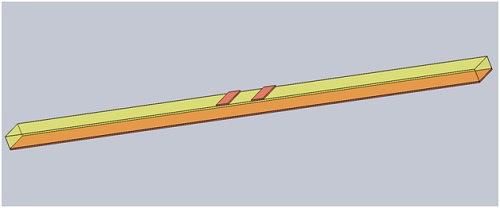
Figure 6 - 1/20 of the structure is modeled for AC Magnetic analysis
In a manner akin to the Magnetostatic analysis, the two traces are modeled as coils for the AC analysis. To incorporate the skin depth effect in the AC resistance calculation, the coils are modeled as solids, as wound coils do not accommodate eddy currents. Figure 7 displays the AC resistance values for frequencies ranging from 1 KHz to 1 MHz, as computed by EMS and compared to Reference [1]. Meanwhile, Figure 8 presents the AC inductance results and their comparison over the same frequency range.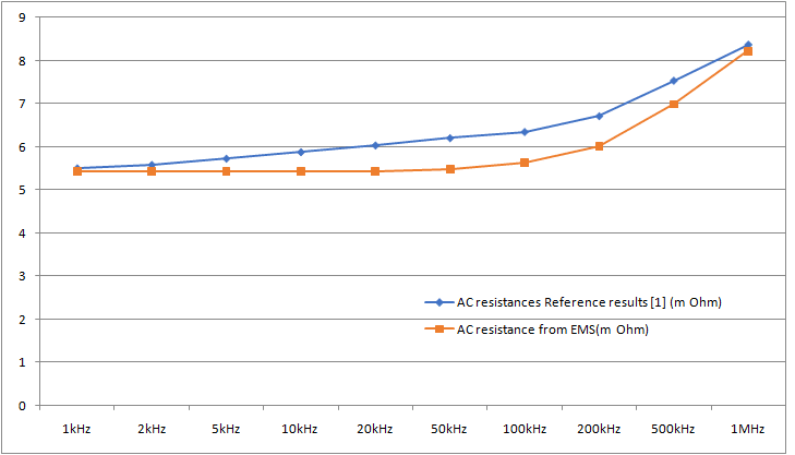
Figure 7 - AC resistance computed by EMS and compared to Reference [1]
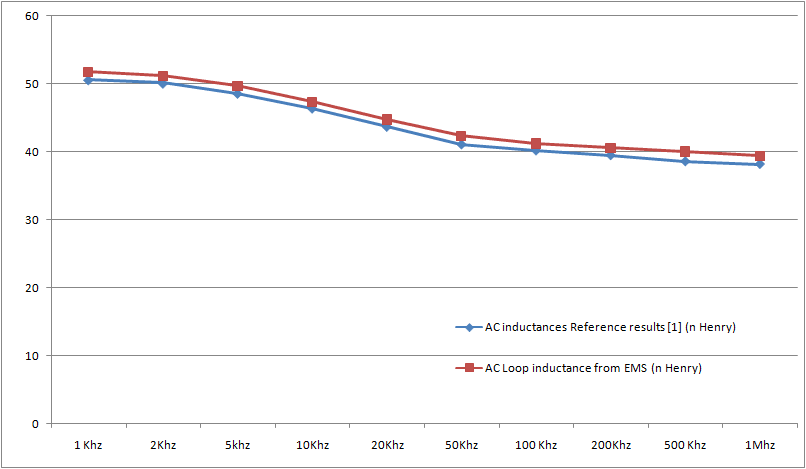
Figure 8 - AC inductance computed by EMS and compared to Reference [1]
Conclusion
This blog note delves into the significance of accurately simulating parasitic parameters in PCB designs using EMS, addressing a critical concern for electronic design automation professionals. By providing a detailed examination of EMS's capabilities in capturing the nuanced electrical properties of PCBs, this note affirms the tool's precision in parasitic capacitance, resistance, and inductance calculations. This insight not only bolsters confidence in high-frequency circuit modeling but also underscores EMS's indispensable role in advancing electronic design and optimization, positioning it as a vital resource for engineers tackling the complexities of electromagnetic interference.