Crossovers
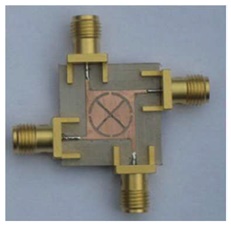
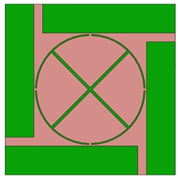
In monolithic Integrated Circuits (IC) and antenna arrays, crossovers play a crucial role in maintaining signal purity at transmission line intersections. Among various types, printed planar crossovers are popular for their compact and simple structure. In this article, we design and simulate a compact planar crossover using the full wave 3D simulator HFWorks. An S Parameter analysis explores its electromagnetic behavior, as shown in Figure 1, depicting the fabricated prototype.
The Model Geometry
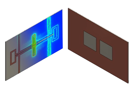
This compact planar crossover consists of a square micro-strip patch excited by four perpendicular micro-strip lines. The square patch includes two perpendicular rectangular slots and four arc-shaped slots, resonating at 2.4 GHz. With dimensions approximately 13 mm x 13 mm x 0.64 mm, as illustrated in Figure 2.
The square patch crossover is built on a dielectric substrate with a relative permittivity of 10.2. The substrate sits atop a very thin layer, treated as a perfect electric conductor (PEC) surface. Surrounding the crossover is an air box. Key structure parameters are outlined in Table 1.
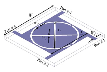
| Parameter | Value (mm) |
| W | 13 |
| W1 | 0.2 |
| W2 | 0.2 |
| Wf | 0.67 |
| L | 8.6 |
| L1 | 8.4 |
Simulation Setup
The Scattering Parameter simulator was employed, utilizing a frequency plan defined with a fine step uniformly distributed between 2 and 3 GHz.
The design incorporates 4 wave ports, applied to small areas adjacent to the micro-strip line's starting and ending points. The ground metal is treated as a Perfect Electric Conductor.
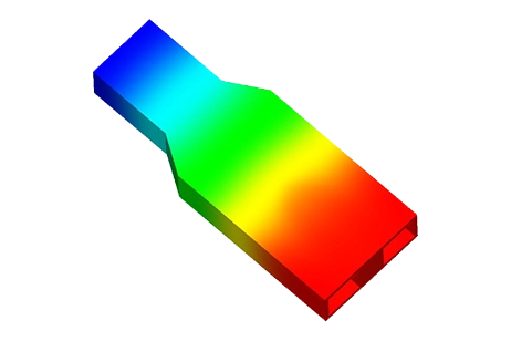
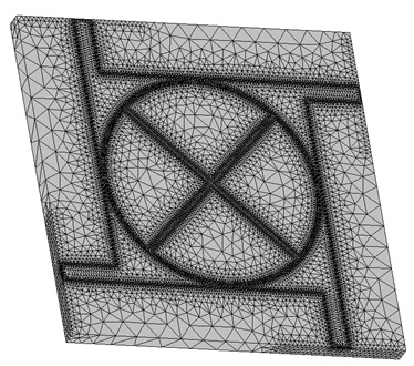
Meshing
A fine mesh is necessary for the ports and conductor edges, as well as for the slots within the patch. The meshed structure is depicted in the figure below.
Simulation Results
To validate the accuracy of HFWorks, we compare its simulated S-parameter results (S11, S21, and S31) with measured data from the square patch crossover, as depicted in the following figure.
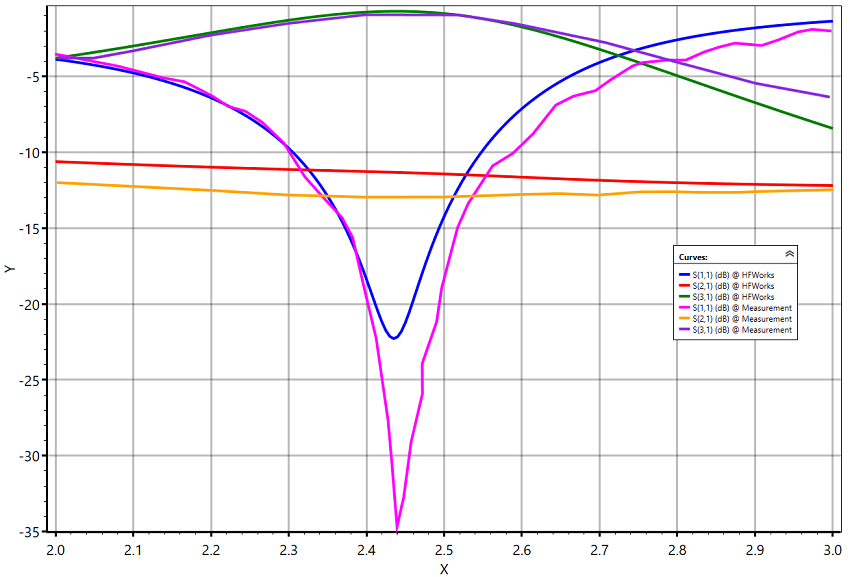
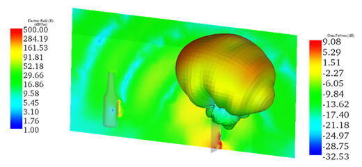
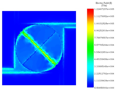
The return loss exceeds 10 dB within the 2.3 - 2.54 GHz range, with an insertion loss below 1 dB. Isolation surpasses 13 dB, as demonstrated in Figure 5. Both simulated and measured results exhibit a bandwidth of 12% centered at 2.4 GHz. HFWorks automatically computed the electromagnetic field, illustrating the electric field distribution at the resonance frequency of 2.4 GHz, with an incident power of 1W, as shown in Figure 6.
Conclusion
In this application note, a compact planar crossover for monolithic Integrated Circuits (IC) and antenna arrays is designed and analyzed using the full wave 3D simulator HFWorks. The crossover, characterized by its square microstrip patch design with perpendicular slots and arc-shaped slots, operates effectively at 2.4 GHz. Its compact dimensions and the use of a dielectric substrate with a high relative permittivity ensure a minimal footprint while maintaining signal integrity. Simulation results reveal that the crossover achieves a return loss greater than 10 dB and an insertion loss below 1 dB within the 2.3 - 2.54 GHz range, demonstrating excellent isolation of over 13 dB. The simulated and measured S parameters align closely, validating the accuracy of HFWorks in predicting electromagnetic behavior. Additionally, the electromagnetic field distribution at 2.4 GHz, with an incident power of 1W, was successfully visualized, highlighting the crossover's efficiency in signal transmission and its potential application in beam-forming networks and other advanced communication systems.
References
[1] B.Henin, A.Abbosh “Compact Planar Microstrip Crossover Based for Beam-forming Networks” Progress In Electromagnetics Research C, Vol.33, 123-132, 2012.