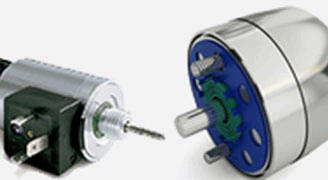
Elevate electromechanical system design with EMWorks, ensuring precision and efficiency in actuators and solenoids.

Revolutionize antenna and radome design with EMWorks' electromagnetic simulation for superior connectivity and protection.

Innovate in biomedical engineering with EMWorks, optimizing medical devices and studying EM exposure impacts.

Advance EV technology with EMWorks' simulations for motor design, charging systems, and EMC.
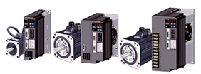
Revolutionize electromechanical designs with EMWorks, mastering the complexities of electrical machines and drives.
Master EMI and EMC challenges with EMWorks, enhancing device safety and performance in diverse sectors.

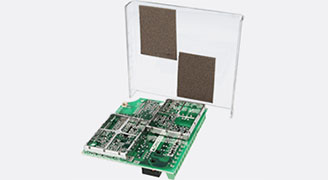
Revolutionize electronic design with EMWorks' EDA tools, optimizing PCBs, EMC, and RF components for superior performance.
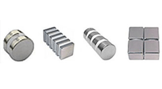
Optimize magnetic fields with EMWorks for magnets and arrays, enhancing performance in various applications.
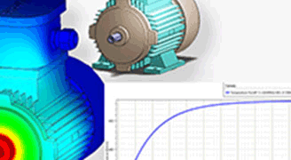
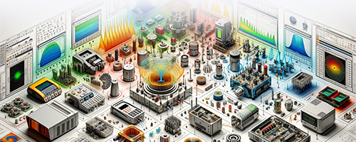
Experience integrated Multiphysics simulations, coupling electromagnetic, thermal, and structural analyses.

Optimize your RF and Microwave components with EMWorks' sophisticated simulation solutions for enhanced performance.
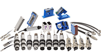
Innovate in Non-Destructive Testing with EMWorks' advanced sensors and NDT/NDE solutions across industries.

Innovate in power engineering with EMWorks. Design efficient transformers and high-voltage components.