This article showcases how HFWorks, integrated with CAD software, streamlines the design and simulation of microstrip to coplanar waveguide (CPW) transitions in hybrid integrated circuits. Utilizing a method that combines microstrip-to-slotline transitions, we present a broadband solution for seamless integration. To mitigate capacitive reactance at lower frequencies, a strategic addition of a short-ended microstrip stub enhances performance. Our simulation highlights the effectiveness of this approach, with Figure 1 displaying the 3D model of the transition, demonstrating the precision and efficiency achievable in modern circuit design.
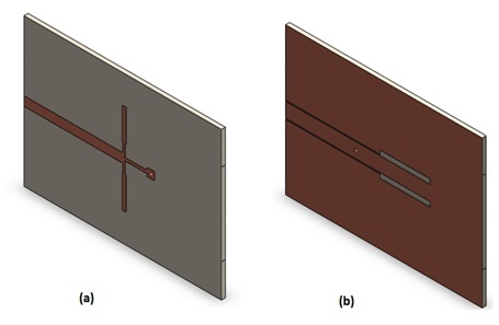
Figure 2 illustrates the detailed layout of the transition from Microstrip to CPW, with key geometrical outcomes compiled in Table 1. This visualization emphasizes the meticulous design process, highlighting the precision and effectiveness of the transition strategy in circuit integration.
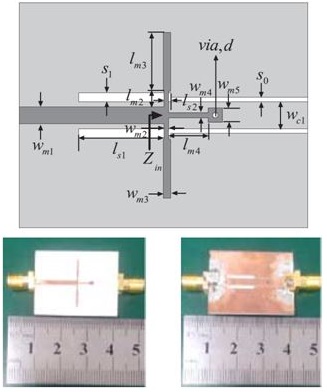
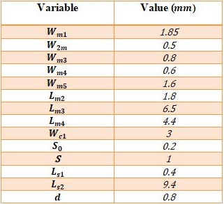
Figure 3 displays a side-by-side comparison of simulated S parameters with actual measurements for a microstrip-to-CPW transition, showing a significant alignment between them. Simulation data shows that the transition achieves a broad bandwidth from 2.05 to 9.96 GHz with a return loss of better than 10 dB, highlighting its wide-ranging efficiency and accuracy.
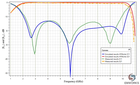
The maximum and minimum insertion losses of the transition passband are 1.7 dB and 0.2 dB, respectively.
This application note explores the design and simulation of a microstrip to coplanar waveguide (CPW) transition using HFWorks, seamlessly integrated with CAD software, for hybrid integrated circuits. By employing a microstrip-to-slotline transition combined with a short-ended microstrip stub, the article presents a broadband solution that effectively mitigates capacitive reactance at lower frequencies, enhancing the transition's performance. The 3D model and detailed layout showcased in the figures illustrate the precision and effectiveness of this design approach in modern circuit integration.
Simulation results reveal a significant alignment between simulated S parameters and actual measurements, confirming the transition's broad bandwidth from 2.05 to 9.96 GHz with a return loss better than 10 dB. Such results underscore the transition's wide-ranging efficiency and accuracy, with the maximum and minimum insertion losses within the passband being 1.7 dB and 0.2 dB, respectively. This analysis not only highlights the potential of integrating microstrip and CPW in hybrid circuits but also demonstrates the capability of advanced simulation tools in achieving high-performance and broadband solutions in modern electronics design.
[1] Ziwen Tao" Broadband Transition Design From Microstrip to CPW", IEEE Microwave and Wireless Components Letters, vol. 25, NO. 11, November 2015, pp 712-714.
| Share on |