Three-dimensional through-silicon-via (TSV) technology enhances chip performance, reduces latency, and minimizes power consumption by establishing direct connections between different layers within a die-stack through the substrate. TSVs, typically 5 to 150 µm in diameter and 20 to 200 µm in length, offer an efficient interconnection method, enabling more compact chip designs compared to traditional wire bonding techniques. Although not widely used in memory and image sensors due to thermal and cost challenges, Xilinx demonstrated successful implementation of 28 Gbps field-programmable gate array (FPGA) systems using a 2.5D architecture with TSV-based silicon interposers. This article aims to model and evaluate the performance of individual TSVs using HFWorks, focusing on S-parameters analysis for thorough simulation.
Figure 2 depicts the TSV connector setup, where a TSV is enclosed within a silicon box, surrounded by an air box within the HFWorks environment. The silicon box has a defined resistivity of 10 ohm·cm. The TSV is represented as a copper bar with a length of 50 µm and a cross-sectional diameter of 5 µm.
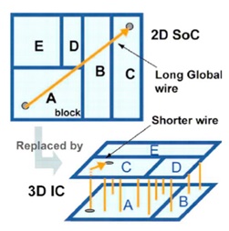
Figure 1 - Wire connections comparison between 2D IC and 3D IC.
A 0.5 µm thick layer of silicon dioxide is applied to insulate the TSV from the substrate. The top and bottom plates of the TSV serve as wave ports, applying excitations with an impedance of 50 Ohms.
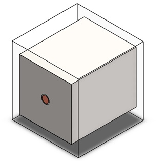
Figure 2 - The 3D model of the Through Silicon Via TSV.
The schematic diagram of the TSV connector is depicted in Figure 3, while the geometric parameters and materials utilized are outlined in Table 1.
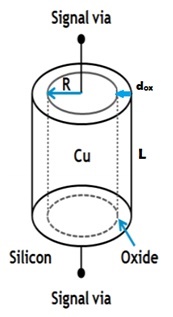
Figure3 - Schematic digaram of a single TSV
Table1 - Dimensional details of the connector
| Parameters | Value | Parts | Materials |
| R | 2.5 ?m | TSV body | Copper |
| dox | 0.5 ?m | Dielectric | Silicon Dioxide |
| L | 50 ?m | Silicon box | Silicon |
| Air Box | Air |
The variations in the S parameter S11 are depicted in Figure 4. As expected, it exhibits a minor insertion loss at high frequencies, primarily attributed to the presence of three fundamental modes within the structure: the slow-wave mode, dielectric quasi-TEM mode, and skin-effect mode. The sharp slope in the graph indicates the transition from the slow wave to the quasi-TEM mode.
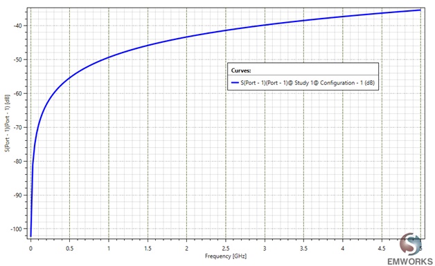
Figure4 - Return loss S11 of the single TSV
The insertion loss graph for S21 shown in Figure 5 demonstrates that the input signal experiences attenuation of less than 0.00005 dB at 1 GHz. This result is favorable as we anticipate S21 to be close to 0 in such scenarios.
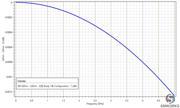
Figure5 - Insertion loss S21 of the single TSV
The distribution of the electric field at 1 GHz is visualized in Figure 6. It's evident that the electric field is uniformly distributed along the fault-free TSV within the substrate

Figure6 - Distribution of the electric field at 1GHz of the single TSV
In conclusion, this application note highlights the significant role of through-silicon-via (TSV) technology in revolutionizing chip design and integration. TSVs offer a promising pathway to enhance chip performance, reduce latency, and minimize power consumption by establishing direct interconnections between different layers within a die-stack. Despite challenges such as thermal issues and cost constraints, advancements in TSV-based architectures, exemplified by Xilinx's successful implementation of 28 Gbps FPGA systems, demonstrate the potential for overcoming these obstacles. The study focuses on modeling and evaluating individual TSVs using HFWorks, employing S-parameters analysis to comprehensively assess their performance characteristics. Results indicate minimal insertion loss and signal attenuation, coupled with uniform electric field distribution along the TSVs. This underscores the efficacy of TSVs in facilitating efficient signal transmission and interconnection within semiconductor devices. By leveraging advanced simulation techniques and optimization strategies, designers can harness the full potential of TSV technology to drive innovation and efficiency in chip design. Ultimately, TSVs represent a key enabler for advancing semiconductor technologies and realizing the vision of more compact, powerful, and energy-efficient electronic systems.
[1] Gong, Zheng, "TSV Equivalent Circuit Model using 3D Full-Wave Analysis" (2014). Electronic Theses and Dissertations. Paper 5238.
| Share on |